


19th February 2021

“Let's run out now, to greener fields, where shines a bright new Sun.
We have a dream, a wondrous dream, that gets the best things done.
A wide blue sky is in our heart now,
Open-ness in our soul,
We'll run together going onwards now,
On towards our goal.
Ahhhh Fujitsu, oh tomorrow is our goal.
Let’s join our hands, with everyone, and smile at each new hour.
We have a dream, an endless dream, of youthful love and power.
We want to use all our skill now,
All the strengths unfurled,
We plan uniting all our new techniques,
Over all the world.
Ahhhhh Fujitsu, forges links all over the world.
Let's make a bond, from heart to heart, throughout the human race.
An unseen power, now in our grasp, can even conquer space.
We want to find a new harmony,
Both in work and play,
We'll share the fresh things we discover now,
Building a new day.
Ahhhhh Fujitsu, Gives a joy with every new day!”
English version of Fujitsu’s company anthem, circa 1990
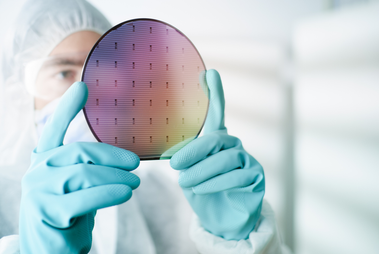 I have not always been a fund manager, thirty years ago I worked for Fujitsu making silicon chips for a living. Back then Japanese semiconductor companies were in ebullient mood. Fujitsu, then the world’s second largest computer company, after IBM, was one of those companies. Fujitsu acquired the British computer company ICL in 1990 and, at the same time, was in the process of building its first silicon chip factory outside of Japan. The factory was built on a site in the North East of England, just outside of Newton Aycliffe, chosen for its proximity to cheap labour and clean water. The closure of the region’s traditional shipbuilding and coal mining industries meant there was an abundance of workers willing to staff the arduous 24-hour shift patterns, required in the semiconductor industry. The giant Kielder Water reservoir was also close enough to supply the factory with the huge quantities of high-quality water required to clean the silicon wafers between the many manufacturing stages. A hefty dose of state aid, from the British government, also helped.
The factory at Newton Aycliffe was a copy of another of Fujitsu’s semiconductor factories, built a few years previously, in Iwate, a town in the North East of Japan. In order to commission the factory and then run the manufacturing process Fujitsu recruited a team of British engineers, who were sent to the Japanese sister factory for training. I was lucky enough to be one of those engineers. I was assigned to the Ion Implantation and Diffusion department.
The electrical circuits in silicon chips are manufactured on the surface of circular discs of single crystal silicon, known as silicon wafers. The Fujitsu factory used six-inch wafers; today much larger twelve-inch wafers are common-place. Silicon’s unique chemical and electrical properties make it the ideal material for making electronic circuits. In its pure form silicon does not conduct electricity, but the energy levels of its electrons are such that, with a little judicious contamination of the silicon crystal, it can easily be turned into an excellent conductor – hence the term semiconductor. The contaminants, known as dopant, we used to make the silicon conduct were atoms of boron, phosphorus and arsenic, which were fired into the surface of the wafer using ion-implantation machines; essentially small particle accelerators that work similarly to an old-fashioned cathode-ray television.
Silicon can also be made into an excellent electrical insulator by baking the silicon wafers, at very high temperatures, in an oxygen rich environment. The oxygen atoms diffuse into the surface of the silicon wafers forming a thin layer of silicon dioxide. Silicon dioxide, otherwise known as quartz, is an insulator.
It is the ability to convert silicon into an electrical conductor with doping and into an insulator with oxidisation which makes it useful for building electrical circuits. The art of making a silicon chip is in forming electrical devices, on the surface of the wafer, by controlling which parts of the surface are converted into conductors, with dopant, and which parts are turned into insulators, through oxidization. Once this is done the resulting devices must be connected with a mesh of fine metallic wires printed on top of the wafer’s surface.
To be fair, it is a bit more complex. Conductors and insulators on their own cannot be used to build a computer. In order to do that you need more complex electronic devices such as capacitors, which can hold a charge acting as memory devices and transistors, which act as switches to build logic circuits.
Capacitors can be built up as a sandwich of conductive and insulating layers deposited on the surface of the silicon wafer. While transistors can be made by selectively doping adjacent regions of the silicon with different atoms. Silicon doped with a sprinkling of boron atoms will conduct electricity through the flow of positively charged electron holes and is known as P-type semiconductor. Silicon doped with arsenic will conduct electricity through the flow negatively charged electrons and is known as an N-type semiconductor. Regions where P-type an N-type silicon come together is known as a P-N junction or a diode, and when a pair of P-N junctions are formed side-by-side you have a transistor. The logic circuits of modern computers require a lot of transistors; one of NVIDIA’s new GPU chips has 54 billion transistors, all of which have to be wired together.
Controlling which areas of the wafer become P-type and which become N-type semiconductor, and then how those areas are connected, is achieved using a photographic process - photolithography. At different stages of the manufacturing process the silicon wafer is turned into a photographic plate. The disc is covered with a light sensitive chemical – photoresist – and an image of the desired electrical components or electrical circuit is projected onto the wafer. The wafer is then developed, like a photograph, to wash away either the exposed or unexposed areas of the photoresist. The photoresist left behind then selectively protect parts of the surface of the wafer from subsequent etching or doping processes.
Making silicon chips is one of the few industries where good engineering and good economics go hand in hand. The smaller you can make your chips the more chips you make on each silicon wafer. At the same time, smaller chips work faster, consume less power and are more reliable. As a result, both the economic and engineering success of the semiconductor industry is driven by one key variable: the smallest feature size that can be projected, onto the wafer, by the lithography systems. This minimum feature size is referred to as the linewidth – the width of the narrowest achievable electrical wire connecting the transistors together.
When we built Fujitsu’s factory, 30 years ago, we used lithography machines capable of printing details as small as 0.5 Microns. This meant it was possible to run 1000 individual electrical wires across each millimetre of the silicon surface (0.5 Microns for the wire and 0.5 Microns for the insulating gap between the wires). Things have moved on since then. Taiwan Semiconductor, now the world’s leading chip manufacturer, expect to be producing chips with line widths of just 5 Nanometers next year. This will allow them to run 100,000 wires per millimetre.
Back in 1975, Gordon Moore forecast the number of transistors on a silicon chip would keep doubling roughly every two years. Moore’s forecast became known as Moore’s law and has largely held true since 1975. One of the companies at the forefront of keeping Moore’s law on track is ASML, currently the world’s leading manufacturer of the photolithography machines.
The key barrier to printing ever narrower line widths comes from the nature of light itself. Light is made of electromagnetic waves, with different coloured light having different wave lengths. When the wavelength of the light becomes comparable to the width of the lines being printed, the projected images become too blurred to define the shapes of the circuits. In order to get around this problem, engineers have had to build photolithography machines with special light sources producing only high energy – short wavelength – light. Thirty years ago, we used ultraviolet light to project the electrical circuits. Today’s cutting-edge machines require extreme ultraviolet or soft x-ray light. Producing such light is very difficult – ASML have achieved it by using a high-powered pulsed CO2 laser to generate a high temperature plasma of tin atoms which emit the required extreme ultraviolet light. Focusing this type of light is even more difficult because it does not pass through conventional optical lenses. For this reason, it is necessary to focus the light with mirrors and reflect the required image onto the silicon wafer. The engineering needed to achieve this, reliably in a production environment, is phenomenology complex and extremely expensive.
ASML is the only company able to make lithography machines with this soft X-ray capability and TSMC the only company able to use those machines to produce chips with 5nm line widths. There is growing a worldwide shortage of production capacity for manufacturing with this technology and an increasing realisation by Western governments that they have fallen behind Asia in this vital technology.
The semiconductor industry is notoriously cyclical and has been in an expansionary cycle for some time. However, the unique combination of technological breakthroughs, increased consumer demand, supply shortages and geopolitical considerations, suggest the semiconductor investment cycle might continue for some time.
Taiwan Semiconductor is currently the largest holding in your portfolio, ASML the second largest. Two of their customers, NVIDIA and Apple, are the third and fourth largest holdings and several other of your investments are also vital parts of the silicon chip manufacturing ecosystem. It is fair to say, you have a significant exposure to this exciting and rapidly expanding industry.
We are very comfortable with the semiconductor industry and anticipate being invested in it for some years to come. That said, despite our love of the technology, we do not view the semiconductor industry through rose tinted glasses. The story of the Fujitsu factory in Newton Aycliffe carries a warning. Just a few years after we built the factory, the economics of the semiconductor industry changed dramatically. The British factory could not compete with up-and-coming Korean and Taiwanese factories, it was closed down in 1998. Many of the people I had worked with back then lost their jobs. Follow this link to hear the local MP, Tony Blair, discussing the factory’s demise. With that experience in mind, as always, if the facts change, we will not hesitate to change your portfolio accordingly.
Incidentally, one of the techniques used in semiconductor manufacturing is known as Statistical Process Control or SPC. This is the process of continually monitoring, measuring and assessing the performance of production process, looking for quantifiable statistical aberrations. SPC is used to quickly take malfunctioning machines out of the production line so that they do not spoil the chips. We use a similar process to monitor and manage your portfolio, and to tell us when we need to change your portfolio. The approach we use is partially inspired by the SPC techniques used in the semiconductor industry.
Finally, to the song at the beginning of the article. It was played over the Fujitsu factory’s speaker system, in Iwate, in the morning as we arrived for work. We would sing along to it as we entered the factory. We were told it was a translation of the company’s anthem, recorded for us.
To join our distribution list send us a message at info@Equitile.com
 Debt & the magical mathematics of Brahmagupta
2
Debt & the magical mathematics of Brahmagupta
2
 Is corporate debt addictive?
2
Is corporate debt addictive?
2
 2016: A Tale of Two Walls
2
2016: A Tale of Two Walls
2
 Revolutionary Fervour
2
Revolutionary Fervour
2
 Reckless Prudence - How to break a pension system
2
Reckless Prudence - How to break a pension system
2
 Monetary Policy on a War Footing
2
Monetary Policy on a War Footing
2
 Still Flashing Green: Equities in a world of higher growth and financial repression
2
Still Flashing Green: Equities in a world of higher growth and financial repression
2
 Public Deficits, Private Profits
2
Public Deficits, Private Profits
2
 Regulating Psychopaths
2
Regulating Psychopaths
2
 Over Easy - Can Monetary Policy Become Self-Defeating?
2
Over Easy - Can Monetary Policy Become Self-Defeating?
2
 Depressed lobsters and the dividend yield trap
2
Depressed lobsters and the dividend yield trap
2
 Build a company on prudence and trust, not debt
2
Build a company on prudence and trust, not debt
2
 A New Maestro? Observations on an important speech by Fed Chairman Powell
2
A New Maestro? Observations on an important speech by Fed Chairman Powell
2
 The unspoken political truth about debt
2
The unspoken political truth about debt
2
 An Impossible Trinity?
2
An Impossible Trinity?
2
 The Anxiety Machine - The end of the world isn't nigh
2
The Anxiety Machine - The end of the world isn't nigh
2
 The Lost Shield? - The small print in Trump's tax plan
2
The Lost Shield? - The small print in Trump's tax plan
2
 When Prophecy Fails - How to ignore doomsday forecasts
2
When Prophecy Fails - How to ignore doomsday forecasts
2
 Hedonism and the value of money - Part I
2
Hedonism and the value of money - Part I
2
 Meerkats and Market Behaviour - Thoughts on October's stock market fall
2
Meerkats and Market Behaviour - Thoughts on October's stock market fall
2
 Revival of the Fittest
2
A creditable recovery
2
Revival of the Fittest
2
A creditable recovery
2
 Hanging the Wrong Contract?
2
Hanging the Wrong Contract?
2
 0
0
 Investment Letter - Eternal Adaptation
2
Investment Letter - Eternal Adaptation
2
 Luddites and the New Social Revolution
2
Luddites and the New Social Revolution
2
 Hedonism and the value of money - Part II
2
Hedonism and the value of money - Part II
2
 Investment Letter - Constant Reformation
2
Investment Letter - Constant Reformation
2
 Modern Monetary Theory - The Magic Money Tree
2
Modern Monetary Theory - The Magic Money Tree
2
 Facts not Opinions
2
Captain Kirk and the science of economics
2
Facts not Opinions
2
Captain Kirk and the science of economics
2
 When Science Fails
2
When Science Fails
2
 Why ownership matters more than ever
2
Why ownership matters more than ever
2
 Tales of an Astronaut - Lessons from the Unknown
2
Register for Updates
12345678
-2
Tales of an Astronaut - Lessons from the Unknown
2
Register for Updates
12345678
-2


.jpg)

